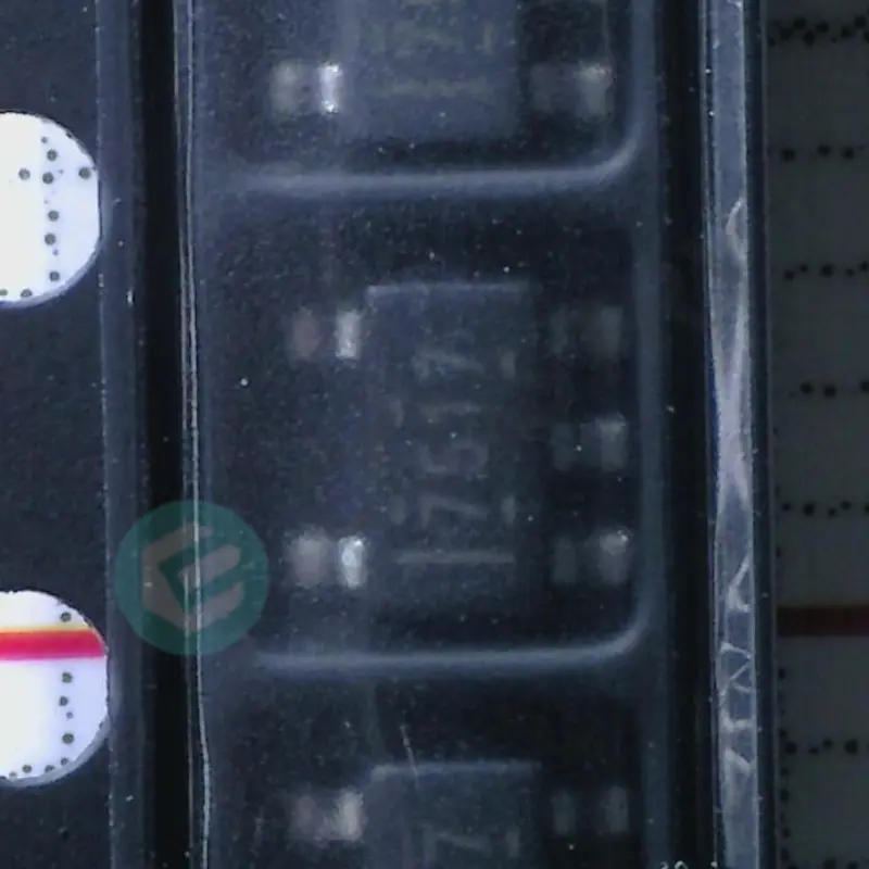
IC GATE DRVR LOW-SIDE SOT23-5


Die Bilder dienen nur als Referenz.
Produktdetails finden Sie in den Produktspezifikationen.
IC GATE DRVR LOW-SIDE SOT23-5
Bei Bestellungen über 200 $ besteht Anspruch auf ein Geschenk im chinesischen Stil in limitierter Auflage.
Bei Bestellungen über 1.000 US-Dollar entfällt die Versandkostenpauschale in Höhe von 30 US-Dollar.
Bei Bestellungen über 5.000 US-Dollar entfallen die Versand- und Transaktionsgebühren.
Diese Angebote gelten sowohl für Neu- als auch für Bestandskunden und sind vom 1. Januar 2024 bis 31. Dezember 2024 gültig.
TI
UCC27517DBVR datasheet
SOT23-5
IC-Chips
 Lead free/RoHS Compliant
Senden Sie jetzt Ihre Angebotsanfrage und wir erwarten, dass wir Ihnen innerhalb von 24 Stunden ein Angebot unterbreiten Mai 06, 2024. Geben Sie jetzt Ihre Bestellung auf und wir gehen davon aus, dass die Transaktion innerhalb dieser Frist abgeschlossen wird Mai 09, 2024. Ps: Die Zeit entspricht GMT+8:00.


1 FEATURES
• Low-Cost, Gate-Driver Device Offering Superior Replacement of NPN and PNP Discrete Solutions
• 4-A Peak Source and 4-A Peak Sink Symmetrical Drive
• Fast Propagation Delays (13-ns typical)
• Fast Rise and Fall Times (9-ns and 7-ns typical)
• 4.5-V to 18-V Single Supply Range
• Outputs Held Low During VDD UVLO (ensures glitch free operation at power-up and power-down)
• TTL and CMOS Compatible Input Logic Threshold (independent of supply voltage)
• Hysteretic Logic Thresholds for High Noise Immunity
• Dual Input Design (choice of an inverting (IN-pin) or non-inverting (IN+ pin) driver configuration)
– Unused Input Pin can be Used for Enable or Disable Function
• Output Held Low when Input Pins are Floating
• Input Pin Absolute Maximum Voltage Levels Not Restricted by VDD Pin Bias Supply Voltage
• Operating Temperature Range of -40°C to 140°C
• 5-Pin DBV (SOT-23) and 6-Pin DRS (3 mm x 3 mm WSON with exposed thermal pad) Package Options
2 APPLICATIONS
• Switch-Mode Power Supplies
• DC-to-DC Converters
• Companion Gate Driver Devices for Digital Power Controllers
• Solar Power, Motor Control, UPS
• Gate Driver for Emerging Wide Band-Gap Power Devices (such as GaN)
3 DESCRIPTION
The UCC27516 and UCC27517 single-channel, high-speed, low-side gate driver devices are capable of effectively driving MOSFET and IGBT power switches. Using a design that inherently minimizes shoot-through current, UCC27516 and UCC27517 are capable of sourcing and sinking high, peak-current pulses into capacitive loads offering rail-to-rail drive capability and extremely small propagation delay typically 13 ns.
The UCC27516 and UCC27517 provides 4-A source, 4-A sink (symmetrical drive) peak-drive current capability at VDD = 12 V.
The UCC27516 and UCC27517 is designed to operate over a wide VDD range of 4.5 V to 18 V and wide temperature range of -40°C to 140°C. Internal Under Voltage Lockout (UVLO) circuitry on VDD pin holds output low outside VDD operating range. The capability to operate at low voltage levels such as below 5 V, along with best in class switching characteristics, is especially suited for driving emerging wide band-gap power switching devices such as GaN power semiconductor devices.
UCC27516 and UCC27517 features a dual-input design which offers flexibility of implementing both inverting (IN-pin) and non-inverting (IN+ pin) configuration with the same device. Either IN+ or IN- pin can be used to control the state of the driver output. The unused input pin can be used for enable and disable function. For safety purpose, internal pull-up and pull-down resistors on the input pins ensure that outputs are held low when input pins are in floating condition. Hence the unused input pin cannot be left floating and needs to be properly biased to ensure that driver output is in enabled for normal operation.
The input pin threshold of the UCC27516 and UCC27517 devices are based on TTL and CMOS-compatible low- voltage logic which is fixed and independent of the VDD supply voltage. Wide hysteresis between the high and low thresholds offers excellent noise immunity.


Request a quote UCC27517DBVR at censtry.com. All items are new and original with 365 days warranty! The excellent quality
and guaranteed services of UCC27517DBVR in stock for sale, check stock quantity and pricing,
view product specifications, and order contact us:sales@censtry.com.
The price and lead time for UCC27517DBVR depending on the quantity required, please send your request to us,
our sales team will provide you price and delivery within 24 hours, we sincerely look forward to cooperating with you.
TI
2884 PCS
OPA1S2385IDRCR .PDF
TI
7888 PCS
OPA1S2384IDRCR .PDF
TI
3479 PCS
OPA197IDBVR .PDF
TI
226 PCS
OPA196IDR .PDF
2024-05-05
Just did a large order with Censtry in China and they were excellent.
2024-05-05
I will give a 5 star.
2024-05-04
Good company to do business .
2024-05-04
Great company. Excellent prices and quality parts.
2024-05-02
Good supplier!!
2024-04-29
Good parts, excellent service, quick shipment. Thanks Katie and Nichole
2024-04-22
I recommend! Fast delivery and high quality product!
2024-04-09
Received the product without any problem. Fast shipping and reasonable prices. I recommend this store.
2024-03-13
Great company to work with, always quotes great and delivers on time...Dean is great!!!
2024-01-20
great company, we wish a great cooperation in the future!

Wir legen großen Wert auf Ihr Feedback. Bitte teilen Sie uns Ihre authentischste Bewertung mit.
*Melden Sie sich bitte an, um einen Kommentar zu veröffentlichen