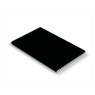
Buffer 2-CH Non-Inverting CMOS 6-Pin TSOP T/R


Die Bilder dienen nur als Referenz.
Produktdetails finden Sie in den Produktspezifikationen.
Buffer 2-CH Non-Inverting CMOS 6-Pin TSOP T/R
Bei Bestellungen über 200 $ besteht Anspruch auf ein Geschenk im chinesischen Stil in limitierter Auflage.
Bei Bestellungen über 1.000 US-Dollar entfällt die Versandkostenpauschale in Höhe von 30 US-Dollar.
Bei Bestellungen über 5.000 US-Dollar entfallen die Versand- und Transaktionsgebühren.
Diese Angebote gelten sowohl für Neu- als auch für Bestandskunden und sind vom 1. Januar 2024 bis 31. Dezember 2024 gültig.
NXP
74LVC2G34GV.125 datasheet
TSOP
IC-Chips
 Lead free/RoHS Compliant
Senden Sie jetzt Ihre Angebotsanfrage und wir erwarten, dass wir Ihnen innerhalb von 24 Stunden ein Angebot unterbreiten Mai 03, 2024. Geben Sie jetzt Ihre Bestellung auf und wir gehen davon aus, dass die Transaktion innerhalb dieser Frist abgeschlossen wird Mai 07, 2024. Ps: Die Zeit entspricht GMT+8:00.


FEATURES
• Wide supply voltage range from 1.65 V to 5.5 V
• 5 V tolerant input/output for interfacing with 5 V logic
• High noise immunity
• Complies with JEDEC standard:
– JESD8-7 (1.65 V to 1.95 V)
– JESD8-5 (2.3 V to 2.7 V)
– JESD8B/JESD36 (2.7 V to 3.6 V).
• ESD protection:
– HBM EIA/JESD22-A114-B exceeds 2000 V
– MM EIA/JESD22-A115-A exceeds 200 V.
• ±24 mA output drive (VCC = 3.0 V)
• CMOS low power consumption
• Latch-up performance exceeds 250 mA
• Direct interface with TTL levels
• Multiple package options
• Specified from −40 °C to +85 °C and
−40 °C to +125 °C.
DESCRIPTION
The 74LVC2G34 is a high-performance, low-power,
low-voltage, Si-gate CMOS device and superior to most
advanced CMOS compatible TTL families.
Inputs can be driven from either 3.3 V or 5 V devices.
These feature allows the use of these devices as
translators in a mixed 3.3 V and 5 V environment.
This device is fully specified for partial power-down
applications using Ioff. The Ioff circuitry disables the output,
preventing the damaging backflow current through the
device when it is powered down.
The 74LVC2G34 provides two buffers.


Request a quote 74LVC2G34GV.125 at censtry.com. All items are new and original with 365 days warranty! The excellent quality
and guaranteed services of 74LVC2G34GV.125 in stock for sale, check stock quantity and pricing,
view product specifications, and order contact us:sales@censtry.com.
The price and lead time for 74LVC2G34GV.125 depending on the quantity required, please send your request to us,
our sales team will provide you price and delivery within 24 hours, we sincerely look forward to cooperating with you.
Adesto
6907 PCS
AT25SL321-UUE-T .PDF
Adesto
6925 PCS
AT45DB081D-SU SL955-AD .PDF
Adesto
7205 PCS
AT45DB081D-SSU SL383-AD .PDF
Adesto
3699 PCS
AT25SF161-MHD-T .PDF
2024-05-02
I hope we can do more buisness in the Future.
2024-05-01
It was a pleasure to work with Susan at Censtry. Thank you
2024-05-01
John Walsh is great to work and is very professional.
2024-04-30
Kevin fast shipper ,RECOMMENDED !
2024-04-29
Lizzeth was a joy to work with.
2024-04-26
Melissa in Censtry Electronics is the best !
2024-04-21
My transaction with Andy was great. He is a nice man and working with him was super easy and fast.
2024-04-10
NICE TO WORK WITH CENSTRY
2024-03-20
Original parts received, good supplier
2024-02-06
Censtry elec, A Great Company
Wir legen großen Wert auf Ihr Feedback. Bitte teilen Sie uns Ihre authentischste Bewertung mit.
*Melden Sie sich bitte an, um einen Kommentar zu veröffentlichen