Clock Drivers & Distribution ISP 0 Delay Unv Fan- Out Buf-Sngl End I


Die Bilder dienen nur als Referenz.
Produktdetails finden Sie in den Produktspezifikationen.
Clock Drivers & Distribution ISP 0 Delay Unv Fan- Out Buf-Sngl End I
Bei Bestellungen über 200 $ besteht Anspruch auf ein Geschenk im chinesischen Stil in limitierter Auflage.
Bei Bestellungen über 1.000 US-Dollar entfällt die Versandkostenpauschale in Höhe von 30 US-Dollar.
Bei Bestellungen über 5.000 US-Dollar entfallen die Versand- und Transaktionsgebühren.
Diese Angebote gelten sowohl für Neu- als auch für Bestandskunden und sind vom 1. Januar 2024 bis 31. Dezember 2024 gültig.
Lattice
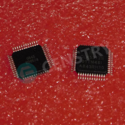
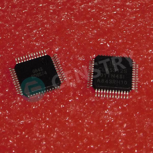
ISPPAC-CLK5312S-01TN48I datasheet
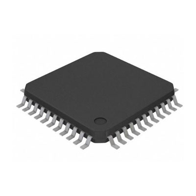
QFP-48
Clock & Timer IC
Senden Sie jetzt Ihre Angebotsanfrage und wir erwarten, dass wir Ihnen innerhalb von 24 Stunden ein Angebot unterbreiten Mai 03, 2024. Geben Sie jetzt Ihre Bestellung auf und wir gehen davon aus, dass die Transaktion innerhalb dieser Frist abgeschlossen wird Mai 08, 2024. Ps: Die Zeit entspricht GMT+8:00.


Features
■ Four Operating Configurations
• Zero delay buffer
• Zero delay and non-zero delay buffer
• Dual non-zero delay buffer
• Non-zero delay buffer with output divider
■ 8MHz to 267MHz Input/Output Operation
■ Low Output to Output Skew (<100ps)
■ Low Jitter Peak-to-Peak (< 70 ps)
■ Up to 20 Programmable Fan-out Buffers
• Programmable single-ended output standards and individual enable controls
- LVTTL, LVCMOS, HSTL, eHSTL, SSTL
• Programmable output impedance
- 40 to 70Ω in 5Ω increments
• Programmable slew rate
• Up to 10 banks with individual VCCO and GND
- 1.5V, 1.8V, 2.5V, 3.3V
■ Fully Integrated High-Performance PLL
• Programmable lock detect
• Three “Power of 2” output dividers (5-bit)
• Programmable on-chip loop filter
• Compatible with spread spectrum clocks
• Internal/external feedback
■ Precision Programmable Phase Adjustment (Skew) Per Output
• 8 settings; minimum step size 156ps
- Locked to VCO frequency
• Up to +/- 5ns skew range
• Coarse and fine adjustment modes
■ Up to Three Clock Frequency Domains
■ Flexible Clock Reference and External Feedback Inputs
• Programmable single-ended or differential input reference standards
- LVTTL, LVCMOS, SSTL, HSTL, LVDS, LVPECL, Differential HSTL, Differential SSTL
• Clock A/B selection multiplexer
• Programmable Feedback Standards
- LVTTL, LVCMOS, SSTL, HSTL
• Programmable termination
■ All Inputs and Outputs are Hot Socket Compliant
■ Full JTAG Boundary Scan Test In-System Programming Support
■ Exceptional Power Supply Noise Immunity
■ Commercial (0 to 70°C) and Industrial (-40 to 85°C) Temperature Ranges
■ 48-pin and 64-pin TQFP Packages
■ Applications
• Circuit board common clock distribution
• PLL-based frequency generation
• High fan-out clock buffer
• Zero-delay clock buffer
General Description
The ispClock5300S is an in-system-programmable zero delay universal fan-out buffer for use in clock distribution applications. The ispClock5312S, the first member of the ispClock5300S family, provides up to 12 single-ended ultra low skew outputs. Each pair of outputs may be independently configured to support separate I/O standards (LVTTL, LVCMOS -3.3V, 2.5V, 1.8, SSTL, HSTL) and output frequency. In addition, each output provides independent programmable control of termination, slew-rate, and timing skew. All configuration information is stored onchip in non-volatile E2 CMOS® memory.
The ispClock5300S devices provide extremely low propagation delay (zero-delay) from input to output using the on-chip low jitter high-performance PLL. A set of three programmable 5-bit counters can be used to generate three frequencies derived from the PLL clock. These counters are programmable in powers of 2 only (1, 2, 4, 8, 16, 32). The clock output from any of the V-dividers can then be routed to any clock output pin through the output routing matrix. The output routing matrix, in addition, also enables routing of reference clock inputs directly to any output.

Request a quote ISPPAC-CLK5312S-01TN48I at censtry.com. All items are new and original with 365 days warranty! The excellent quality
and guaranteed services of ISPPAC-CLK5312S-01TN48I in stock for sale, check stock quantity and pricing,
view product specifications, and order contact us:sales@censtry.com.
The price and lead time for ISPPAC-CLK5312S-01TN48I depending on the quantity required, please send your request to us,
our sales team will provide you price and delivery within 24 hours, we sincerely look forward to cooperating with you.
Lattice
3982 PCS
MXO1200C-3MN2C .PDF
Lattice
1 PCS
MC68360AI25VL .PDF
Lattice
159 PCS
MANO MLV5 .PDF
Lattice
138 PCS
MACH435Q-20JC .PDF
2024-05-02
very fast thanks
2024-05-02
Fast shipping
2024-05-02
Goods arrived and work perfectly.
2024-05-01
impossible to find, except here.
2024-04-30
TRANSISTORS ARE GOOD
2024-04-27
Mercancía correcta. Envío rápido. Muy satisfecho.
2024-04-22
Censtry elec = Good company, happy business
2024-04-11
We highly recommend Pinewood Electronics Ltd and are looking forward to our next deal. Darren is very professional and our order was shipped promptly and the parts were good quality.
2024-03-21
Good supplier !i will buy it again ,Nice
2024-02-07
Very proffessional and reliable company. Was a pleasure for me to work with Mara.

Wir legen großen Wert auf Ihr Feedback. Bitte teilen Sie uns Ihre authentischste Bewertung mit.
*Melden Sie sich bitte an, um einen Kommentar zu veröffentlichen