Ultralow Offset Voltage Operational Amplifier


Die Bilder dienen nur als Referenz.
Produktdetails finden Sie in den Produktspezifikationen.
Ultralow Offset Voltage Operational Amplifier
Bei Bestellungen über 200 $ besteht Anspruch auf ein Geschenk im chinesischen Stil in limitierter Auflage.
Bei Bestellungen über 1.000 US-Dollar entfällt die Versandkostenpauschale in Höhe von 30 US-Dollar.
Bei Bestellungen über 5.000 US-Dollar entfallen die Versand- und Transaktionsgebühren.
Diese Angebote gelten sowohl für Neu- als auch für Bestandskunden und sind vom 1. Januar 2024 bis 31. Dezember 2024 gültig.
AD
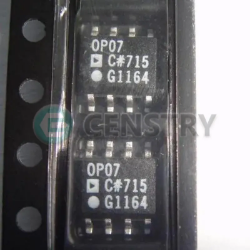
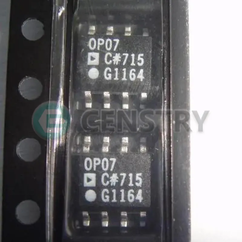
OP07CSZ datasheet
SOP-8
IC-Chips
 Lead free/RoHS Compliant
Senden Sie jetzt Ihre Angebotsanfrage und wir erwarten, dass wir Ihnen innerhalb von 24 Stunden ein Angebot unterbreiten Mai 09, 2024. Geben Sie jetzt Ihre Bestellung auf und wir gehen davon aus, dass die Transaktion innerhalb dieser Frist abgeschlossen wird Mai 14, 2024. Ps: Die Zeit entspricht GMT+8:00.


FEATURES
Low VOS: 75 μV maximum Low
VOS drift: 1.3 μV/°C maximum
Ultrastable vs. time: 1.5 μ
V per month maximum
Low noise: 0.6 μ
V p-p maximum
Wide input voltage range: ±14
V typical
Wide supply voltage range: 3 V to 18 V
125°C temperature-tested dice
APPLICATIONS
Wireless base station control circuits
Optical network control circuits Instrumentation
Sensors and controls
Thermocouples
Resistor thermal detectors (RTDs) Strain bridges
Shunt current measurements Precision filters
GENERAL DESCRIPTION
The OP07 has very low input offset voltage (75 μV maximum for OP07E) that is obtained by trimming at the wafer stage. These low offset voltages generally eliminate any need for external nulling.
The OP07 also features low input bias current (±4 nA for the OP07E) and high open-loop gain (200 V/mV for the OP07E). The low offset and high open-loop gain make the OP07 particularly useful for high gain instrumentation applications.
The wide input voltage range of ±13 V minimum combined with a high CMRR of 106 dB (OP07E) and high input impedance provide high accuracy in the noninverting circuit configuration. Excellent linearity and gain accuracy can be maintained even at high closed-loop gains. Stability of offsets and gain with time or variations in temperature is excellent. The accuracy and stability of the OP07, even at high gain, combined with the freedom from external nulling have made the OP07 an industry standard for instrumentation applications.
The OP07 is available in two standard performance grades. The OP07E is specified for operation over the 0°C to 70°C range, and the OP07C is specified over the −40°C to +85°C temperature range.
The OP07 is available in epoxy 8-lead PDIP and 8-lead narrow SOIC packages. For CERDIP and TO-99 packages and standard microcircuit drawing (SMD) versions, see the OP77.

Request a quote OP07CSZ at censtry.com. All items are new and original with 365 days warranty! The excellent quality
and guaranteed services of OP07CSZ in stock for sale, check stock quantity and pricing,
view product specifications, and order contact us:sales@censtry.com.
The price and lead time for OP07CSZ depending on the quantity required, please send your request to us,
our sales team will provide you price and delivery within 24 hours, we sincerely look forward to cooperating with you.
AD
150 PCS
OP77HSZ .PDF
AD
2747 PCS
OP77GSZ .PDF
AD
68 PCS
OP77GPZ .PDF
AD
100 PCS
OP77FPZ .PDF
2024-05-08
good package ,fast shipping
2024-05-08
excelente servicio pedido en buenas condiciones
2024-05-08
normal Works,thanks
2024-05-07
I have received and mosfets look like good. Fast shipping and delivering.
2024-05-05
Tested. Works fine.
2024-05-02
new relays
2024-04-25
Will continue to source through Censtry Smooth orders and good product.
2024-04-12
We have completed several large deals with Mati and Ilan all went smoothly every time. .
2024-03-16
Censtry elec and his team are honest, reliable. A pleasure to deal with.
2024-01-23
Very professional

Wir legen großen Wert auf Ihr Feedback. Bitte teilen Sie uns Ihre authentischste Bewertung mit.
*Melden Sie sich bitte an, um einen Kommentar zu veröffentlichen